Welcome to Shenzhen Sunshine Good Electronics Co.,Ltd.!


I. Classification by PCB Functional Positioning
1. Flexible Connector Cable Function
Functional Positioning: Transmits ordinary/high-speed/microwave signals or currents under specific power supply in bendable structural spaces.
Layer Structure: Single-layer, double-layer, or multi-layer circuits (generally ≤4 layers).
PCB Wiring: No vias in bending areas; minimal SMD design (backside reinforcement required if necessary); parallel straight-line routing; regular bypass routing for specific transmission lines; anti-interference design using large copper sheets, grid copper, special metal materials, or magnetic materials.
Product Notes: Limited multi-functional integration; FFC can be an alternative for low signal transmission requirements; high-performance PI-based FCCL is required for high signal demands (increasing manufacturing control standards); saves device space and reduces electronic product weight.

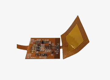
2. Integrated Flexible Sensor Carrier & Cable Function
Functional Positioning: Combines flexible connector cable functions with specific sensor capabilities (eg,photoelectric, temperature, or pressure sensing) to form a functional circuit carrier with a small number of SMD components.
Layer Structure: Single-layer, double-layer, or rarely multi-layer FPC (generally ≤6 layers) and rigid-flex PCBs.
PCB Wiring: Based on flexible connector cable design, integrated with simple carrier manufacturing experience and enhanced product reliability guidelines.
Product Notes: Enables relatively independent functional modules; requires compliance with specific flexible component standards and FPCB/R-FPCB/FPCBA/R-FPCBA manufacturing control criteria. Potential printhead module innovation: High-temperature graphene replacing ceramic sheets, integrated with thermal film resistors to form flexible heating & temperature sensing assemblies.

3. Embedded Integrated Module Substrate Function
Functional Positioning: Integrates flexible connector cable functions with additional circuits (eg, main control, display, or intelligent features) for integrated multi-functional implementation.
Layer Structure: Double-layer FPC, multi-layer FPC, or multi-layer rigid-flex PCBs.
PCB Wiring: Based on flexible connector cable design, integrated with multi-functional carrier manufacturing experience and enhanced functional guarantee, defect control, and reliability design.
Product Notes: Not suitable for high-density functional carriers, but meets rigid PCB board-level manufacturing standards. Currently rarely used in printer terminals.

II. Classification by PCB Special Processes
1. Irregular Shape Process
Functional Guarantee: Ensures optimal positioning of optocoupler sensors, prevents signal reflection; complex structure and high dimensional precision requirements.
Process Description: Shape cutting via laser cutting or die stamping.
Common Issues: Complex molds; burrs, defects, or deviations due to improper material/process selection.
Optimization Solutions: CAM design optimization for FPCB manufacturing; cost-effective mold design; strict adherence to laser/die-cutting operating guidelines; reduced structural complexity through improved photoelectric transmission design.

2. Gold Finger Connection Process
Functional Guarantee: Enables stable signal output and repeated insertion/extraction with printer motherboard connectors.
Process Description: Surface treatment via hard gold plating or electroless nickel immersion gold (ENIG).
Common Issues: Dimensional tolerances, edge position deviations, poor contact, or low wear resistance.
Optimization Solutions: CAM design optimization; cost-effective mold selection; adoption of alternative cost-efficient alloy surface processes (new technologies under performance validation are available in the supply chain).

3. Bump Connection Process
Functional Guarantee: Ensures consistent contact height of multiple contacts in detachable structures, withstanding specific touch pressure and stable signal transmission.
Process Description: Post-FPCB processes including die-stamped bumps, SMT-mounted metal bump components, or synthetic metal adhesive molding bumps.
Common Issues: High cost of SMT-mounted metal bumps; high manufacturing difficulty of synthetic adhesive bumps; potential deformation of die-stamped bumps; uneven contact surfaces.
Optimization Solutions: Die-stamped bumps offer the best cost-performance; SMT-mounted metal bumps are easy to design/manufacture; synthetic adhesive bumps provide the highest stability despite higher complexity. Exploration of new processes is ongoing.

4. Characteristic Impedance Control Process for Modular PCBs
Functional Guarantee: Reduces loss and interference in high-speed signal transmission.
Process Description: Systematic processes including rigorous design, material selection, line width/spacing control, thickness (absolute/relative) control, and performance testing.
Common Issues: Unstable material dielectric constant; improper line width; imprecise layer structure; impedance mismatch caused by uncontrollable thickness.
Optimization Solutions: Process compensation for line width; etching parameter control; inner-layer line width/defect control; consideration of solder mask thickness impact on characteristic impedance (Z0).